
May 2014 Newsletter: Volume 1, Issue 2
A Message From the Director, Jian-Ping Wang
Welcome to the second C-SPIN quarterly Newsletter. We have two short and exciting research stories about cross-theme collaboration, one of the keys to the success of our Center. For me, these stories show how much fun it is to work with C-SPIN PI teams. Thanks to Mike Lotti for his efforts in putting the Newsletter together.
Reflections on my meetings with PIs. Thanks to all the PIs for opening their minds and sharing with me during the one-on-one discussions in December and January. I learned a lot of exciting things beyond what I saw in the Annual Review Power Point presentations, and I also heard about issues that could lead to an inefficient research center if we ignore them (as many large centers do). I also appreciated the opportunity to pass on the expectations of our sponsors, the C-SPIN management, and the C-SPIN Theme leaders.
Student/Postdoctoral fellows mini-workshop. C-SPIN never stops trying new ways to engage our students in interdisciplinary learning. We sponsored the first C-SPIN Students/Postdoctoral fellows mini-workshop on March 16. Students and postdocs presented at the workshop and discussed several issues related to spintronics research – all without any PIs present! Thanks to Marie Rahne for helping me organize this and C-SPIN postdocs Dr. Mahdi Jamali and Dr. Alan Kalitsov for chairing the workshop. The second mini-workshop will be held on May 14 and 15 – and again, no PIs allowed!
Midterm review on May 12 and 13. All PIs will present their exciting research at this meeting, but I also expect them to challenge each other and to face challenges from their colleagues. Several breakout sessions will be dedicated to discussing ways PIs can work together efficiently on several topics: spin device fabrication and feasibility demonstrations, new spin device concepts, topological insulators and related devices, and new spintronics materials. All presentation materials will be sent to our sponsors and uploaded to SRC website.
Seeing What's There Transmission
- Electron Microscopy and C-SPIN
A Note from Jian-Ping Wang: Within C-SPIN, we have access to two of world's best TEMs: one at the University of Wisconsin-Madison, and one at the University of Minnesota. Below, Paul Voyles and Andre Mkhoyan, two "masters" of materials interface issues, explain what we have learned with these microscopes and what we hope to accomplish with TEM in the year ahead.
Paul Voyles
In the computer world, it's been said that "the interface is the device." In other words, if different materials don't function well (or at all) when put together, the device fails. When we make a new device, then, we have to find out what's going on at the interfaces, and for C-SPIN that generally means three things: 1) Seeing if we've made what we hoped to make, 2) Determining an interface's spintronics properties, and 3) Seeing the exact structure of the interface so that we can develop theoretical explanations of those properties. Only TEM enables us to "see" the interface in enough detail to accomplish these goals and, eventually, move toward making viable spin-based transistors.
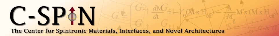
In 2013, this meant a C-SPIN Theme 3 work flow which went something like this. Over the course of the year, Chris Palmstrøm made nearly 20 samples of a Co2MnSi – GaAs interface at UC-Santa Barbara and sent them to Paul Crowell for spin property measurements at the University of Minnesota. When I got the samples from Paul Crowell, I used the TEM here at the University of Wisconsin-Madison to image and measure the interface. (See the picture to the left). Paul Crowell and I sent our data to Bill Butler at the University of Alabama so he could develop a theoretical model of the interface and its properties. At the Annual Review last September, Bill Butler presented some initial work based on our findings, and now we're working together to refine the model and our collective understanding of the science and technology of this interface. We expect this work flow to continue throughout 2014 and 2015.
We were fortunate that some of this work was underway before C-SPIN began in 2013. In particular, a method for evaluating spin channel materials was in place because of the long-term collaboration of Chris Palmstrøm and Paul Crowell. But the Center's funding and organization has definitely sped up the process of collaboration and refinement – which is, of course, exactly what Centers like C-SPIN are supposed to do.
I have also begun to study Cr2O3 films for Theme 2 with Christian Binek of the University of Nebraska. These films are magnetoelectric, which means that their magnetic state can be switched with an electric field as well as a magnetic field. Christian has used this property to create a device that stores information using magnetism, but that can be switched using an electric field instead of an electric currents or a magnetic field, both of which demand much more of energy. The problem, though, is that when we grow thin films of the same material, which we need for real electronic components, it is much harder to switch the magnetic state. We guess that this is due to crystal defects which are common in thin films, but we don't know yet which ones are most important. Thus far, I have measured four Cr2O3 samples, and we hope to understand how to grow high performance thin films by the end of the year.
It's also likely that I will measure some magnetic nanostructures for Theme 1 in 2014, and I'm certainly expecting to analyze samples that may not be on anyone's radar right now. We're on the forefront of groundbreaking science, after all, so surprises are the rule, not the exception.
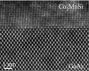
Andre Mkhoyan
The new STEM at the University of Minnesota will be an incredibly valuable tool for C-SPIN. Actually, it already has been a valuable tool.
But first, the specifics. The microscope's official title is FEI Aberration-Corrected and Monocromated Titan 60-300 Scanning and Transmission Electron Microscope, and it can picture samples at a sub-0.1nm (or sub-1Å, if you prefer) resolution.
But high resolution is only part of this microscope's unique power. It also allows us to do extraordinarily fast and accurate spectroscopy. By exciting the electrons in the sample and measuring their return to their normal energy states, we can quickly identify the atoms in the sample. In other words, we can directly "see" the individual atoms inside the crystals at interfaces and know which atoms are out of place in crystal structures. In my opinion, it will be a while before the world sees a substantially better microscope.
 Prof. Andre Mkhoyan at the newly installed at the University
 of Minnesota aberration- corrected and monocromated
FEI Titan STEM. Credit to: Frank Snowden, CEMS-UMN
This does not mean, however, that the TEM at the University of Wisconsin-Madison is now defunct for C-SPIN. Far from it. Paul Voyles and I estimate that 90% of C-SPIN's electron microscopy work can be done with either microscope. In other words, having two microscopes means than we can get nearly twice as much imaging done, and there is more than enough TEM work in C-SPIN to keep both of our groups busy in the coming years. I expect we will be using the new HR-STEM for C-SPIN materials at least once per week for the rest of 2014 and 2015, and I'm sure that the TEM at the University of Wisconsin-Madison will be just as busy.
It's also worth pointing out that, when it comes to highly technical work, people are more important than equipment. In the context of C-SPIN, this roughly means that our sub-specialties dictate the division of labor: Paul Voyles' group works on 3D materials, and my group generally works on 2D materials.
The HR-STEM at the University of Minnesota became fully operational in February. Since then, my group has used it to measure two spin channel materials for Theme 2: MoS2 and WS2, both from Ludwig Bartels and Cengiz Ozkan at UC-Riverside. Much of our work has been dedicated simply to getting good samples, but we have also learned a lot about these materials. We will continue to image Theme 2 samples from UC-Riverside in 2014 and 2015.
Jian-Ping Wang expects that new magnetic tunnel junction materials will be ready for HR-STEM analysis this year, Steve Koester is sure to provide a steady supply of additional Theme 2 samples, and I'm sure that other C-SPIN scientists will be requesting time on the microscope as new materials get developed. In other words, I expect my group to be busy with the HR-STEM in 2014 and 2015. Perhaps more importantly, I aim to constantly improve C-SPIN's procedures for making and handling samples so that contamination is minimized and quality time on the HR-STEM is maximized. The more we can get good samples to the HR-STEM, the more we can move the science of C-SPIN forward and start to build a real spin-based computer.
 Prof. William Butler
Q&A with William Butler, University of Alabama, Theme 3 Leader
A Note from Jian-Ping Wang: When I was thinking about putting together a team of scientists for a spintronics research center, Bill Butler was at the top of my list. I knew of his excellent work as a materials scientist and as the longtime Director of the University of Alabama's Center for Materials for Information Technology, of course. But his groundbreaking work with tunneling magneto-resistance (TMR) and his ongoing passion for understanding magnetic materials made him a "must have" for a spintronics Center.
Q: How did you get interested in working with magnetic materials?
Butler: In the 1960s and 70s, I worked on alloys, trying to understand their resistivity and structure and to calculate their electronic density of states. In the 70s, I also worked on superconductivity – the old fashioned kind where 23K was considered a high Tc – and this involved transition metals. In the 1980s I was interested in transport theory when GMR was discovered. So the combination of alloy theory, transition metals and transport theory led to an interest in transport in magnetic materials.
Q: Describe the research you did before 2013 that has played a role in C-SPIN.
Butler: In 2001, I and colleagues at Oak Ridge National Laboratory predicted that Fe and MgO – that is, a ferromagnetic metal and an insulator with a compatible structure – could be layered in a particular way to make a highly spin-polarized current and generate a large TMR. Our prediction violated the conventional wisdom of the time, but Stuart Parkin at IBM and Shinji Yuasa at AIST applied our theories and were able to generate an order of magnitude higher TMR than had been seen before. It turned out that we were also lucky in that the growth properties of MgO made it a convenient material to work with. We also predicted – again, contrary to the conventional wisdom of the time – that the tunneling resistivity of MgO would be surprisingly low for a wide band-gap insulator. This also turned out to be true and led to Fe, CoFe and MgO becoming the materials of choice for hard drive sensors and are the primary materials being investigated for Spin-Torque MRAM within C-SPIN and elsewhere.
Q: Describe the research you are doing now for C-SPIN.
Butler: I am working on three C-SPIN projects. With my grad students Chocka Sivakumar and Javad Gasheemi and C-SPIN PIs Chris Palmstrøm, Paul Voyles, and Paul Crowell, I'm trying to understand the interface between Heusler alloys and GaAs. GaAs can be used to transport spins, especially at lower temperatures, and Co2MnSi (a Heusler alloy) seems to be particularly good at injecting spins into GaAs. Unfortunately, the interface between these materials is extremely complicated. We are still not sure which atoms are where at the interface or why we see the properties we do. We hope that ongoing characterization – both during growth and with an electron microscope – and first-principles based modeling will help us understand and improve these interfaces. As we come to understand more, we may test other materials as well.
I am also working with Alan Kalitsov, Tim Lovorn and Oleg Mryasov to understand how spin-orbit effects may be used to drive spin-dependent transport and cause magnetic switching. We are particularly interested in topological insulators, which behave as insulators in their interiors but conductors on their surfaces. They are extremely robust and generally good at injecting spin.
A third project that is partly supported by NSF funding involves understanding Heusler alloys. Many of these materials have the interesting property of being metals for one type of electron spin and semi-conductors for the other. We call this kind of material a "half-metal" and we want to understand the "why" behind their properties and make Heusler alloys that fit the needs of spintronics devices. These materials are cubic so they do not have uniaxial anisotropy, but we have some ideas for giving them perpendicular anisotropy while maintaining their half-metallicity.
Q: How has C-SPIN enhanced your own research and the field of spintronics in general?
Butler: C-SPIN has enabled me and my team to collaborate with some of the world’s most talented experimental groups. This has been really exciting and we've made a lot of progress that would have been impossible without such a Center. The challenging goals of C-SPIN have also forced all of the C-SPIN scientists to get out of their comfort zones. It is tempting to take what you know and have had some success with and try to apply it in similar areas and get more papers published. But when you are trying to help a team reach a challenging goal, you are usually forced to face up to problems that you would have otherwise avoided. This is hard and slow, but you also learn new things – which is the reason most of us chose science as a career.
Student and Post-Doc Profiles
 Ashutosh Rath
Ashutosh Rath
Post-Doctoral Researcher at the University of Wisconsin-Madison
I am currently working on analyzing atomic level interfaces between magnetic materials and spin channels using electron microscopy (Theme 3). I work with Paul Voyles to obtain and interpret TEM results.
I am fascinated by electron microscopy because it's such a powerful technique for crystal structure imaging and structure analysis. It's safe to say that the direct visualization of atoms inspired me to continue in the TEM field. Modern aberration-corrected microscopes, which I first came across during my Ph.D. research, are wonderful because they make it possible to resolve inter-atomic distances and to image individual atoms and crystalline defects.
I studied for my Ph.D. in India at the Institute of Physics in Bhubaneswar, which is in the eastern part of the country. My Ph.D. work focused on dynamic and static TEM studies of Au-Si and Au-Ge nanostructures. I was also a postdoctoral research associate at the Indian Institute of Science in Bangalore, where I focused on minimizing the error in the calculation of lattice spacing (HRTEM) of nanoparticles and on growing and characterizing amorphous SiOx nanowire assemblies. All of this was good training for my current work within C-SPIN.
I have published 20 papers and have three pending, all of them containing results from my TEM studies.
 Tim Lovorn
Tim Lovorn
Ph.D. Candidate at the University of Alabama
I am currently working on modeling topological insulator/ferromagnet interfaces for C-SPIN. These interfaces have been shown to generate spin torque with high efficiency, but we need a more detailed picture of the process. Understanding this better could be very useful for creating spin logic devices. This project addresses questions central to Theme 2 and Theme 3.
I am also studying a new microscopic model of cuprate high-temperature superconductors, developed by Sanjoy Sarker, for my Ph.D. dissertation. This model is foundationally similar to some other well-studied cuprate models but is able to account for essential cuprate properties that other models cannot. I have two publications with Dr. Sarker on this topic and a third is in development.
I originally wanted to study high-energy theory, but I was recruited by Dr. Sarker to do cuprate modeling and I haven't looked back. I enjoy exploring the large overlap of theoretical tools used for studying condensed matter and high-energy physics.
I am very inspired by the goal of creating spin logic and would be quite happy to continue working in spintronics. I have developed a skill set at the intersection of quantum field theory, device modeling, and programming which I want to continue exercising and expanding. I am passionate about scientific computing, which is why spin logic is so significant to me. The more the computing platform improves, the more I can do.
