
May 2016: Volume 3, Issue 2
A Message from C-SPIN Director, Jian-Ping Wang
First, I have to say I really enjoyed reading the interview with Dr. Todd Younkin, STARnet program manager. We all have a lot of questions about future information technology: I am sure you will get some answers out of the interview. I would also like to bring to your attention an excellent article in The Economist’s Technology Quarterly, which discusses the challenges of developing future computing technologies. The article includes a lot of interesting discussion related to our work and goals, and highlights the demand for our research.
Second, I would like to share with you that C-SPIN PIs and students have continued to generate exciting results. In particular, Prof. Geoff Beach published his latest research achievement on skyrmions in February issue of Nature Materials, and Prof. Mingzhong Wu published his new discovery of photon-generated spin current based on C-SPIN materials in a recent issue of Nature Physics.
Third, I would like to congratulate our PIs and students who delivered exciting talks at the APS March meeting. Special congratulations go to Prof. Maxim Tsoi, our experimental pioneer on antiferromagnetic spintronics, who presented his latest results in this exciting field. I am also glad to highlight our new PIs: Prof. Jiwei Lu, who has been working on the growth of high quality magnetoelectric materials (e.g. Cr2O3) and novel magnetic metal-insulator-transition materials by a unique sputtering process, and Prof. Kang Wang, who has been working on the implementation of antiferromagnetic materials as part of spin Hall switching devices for memory.
Fourth, I am glad to announce that C-SPIN has been actively involved in STARnet’s materials benchmarking activities, especially Prof. Paul Crowell and Prof. Christian Binek. We will spend more time in the following months coordinating spintronic materials benchmarking with the FAME and LEAST centers. I also would like to thank Prof. Chris Kim and Prof. Sachin Sapatnekar and their students, who have represented C-SPIN and presented three case studies on spintronic devices at STARnet’s Beyond CMOS Benchmarking workshop during the first week of May.
Last but not least, I can’t wait to attend the Topological Insulator Spintronic Devices workshop on May 12 and 13. Pursuing new physics that could lead to revolutionary spintronic devices is one of the key visions for C-SPIN. I believe this workshop will trigger some exciting discussion among the world-leading physicists, materials scientists, electronic device researchers, and industry leaders.
Thanks again, to Mike and Marie for preparing this issue of our newsletter.
Q&A with Todd Younkin, STARnet Program Manager
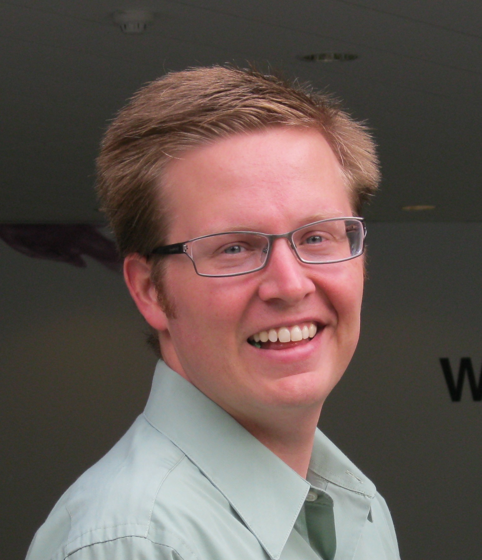 Todd Younkin
Q: What inspired you to temporarily leave Intel and become Program Manager for STARnet?
The SRC’s pre-competitive, external research model has been a critical part of Intel’s success. It has helped to foster world-class research and has led many intelligent, hard-working students to prosperous careers in the semiconductor industry. These folks, in turn, have fueled many of the innovations that are coming down the pipeline or are now in the products we routinely take for granted! So when the opportunity arose early last year to become the STARnet program manager and to help shape a follow-on research engagement with DARPA, it was an opportunity that I couldn’t pass up. It really sold itself.
Q: You've followed the six STARnet centers since they began in Nov. 2012. How have they lived up to STARnet's mission to develop beyond-CMOS technologies and solve complex systems integration problems?
When I was a Ph.D. student (studying organometallic and polymer chemistry), you went into the lab, nurtured a few of your ideas, stumbled across some serendipity that you later tried to explain, and – PRESTO – you emerged from the lab a few years later with a thesis and, hopefully, a job. Seeing how the students from these six STARnet centers collaborate with researchers from other centers, universities, scientific disciplines, etc. is truly inspiring! Today’s students are also able to balance simulations and experiments in a way that would not have been possible just a few short years ago. As a result of this ‘socialized’ and well-balanced research approach, the students from our six STARnet centers have been able to quickly understand and tackle very complex problems that span a wide array of topics: precursors for 2D materials, mm3 sensor nodes, approximate computing, heterogeneous integration, memory-centric computing, and networks of networks, and others. The good news is that the STARnet centers continue to exceed their mandate and have raised the bar above what folks perceived to be possible just a few short years ago. The challenge, of course, is that we are now being asked to innovate at an even faster pace in order to stay competitive against the global research agenda.
Q: What do you hope the STARnet centers focus on with 18 months left to go?
Much like years 4 and 5 in a Ph.D. study, now is the time to realize that things are coming to a close fairly soon. You can’t afford to “dilly-dally.” It is a time to focus, be highly productive, push forward the good ideas, and be cognizant of leaving your legacy. If I were in a STARnet center, I’d ask my colleagues these questions:
- What are the items that the center will be known for?
- What are the key experiments or simulations that need to be completed in order to leave a strong legacy?
- Have we reached out to your industrial liaisons in a while? What do they want to see? What do they consider success?
- Where do talks or publications need to go in order to raise the visibility of our effort?
- What are the ways that we can easily “dot the Is” and “cross the Ts” such that our scope of work is completed?
- What are the things that we proposed that will never work? (and why?) (These are important to document and are highly valuable to our sponsors.)
I believe that these are the kind of items to ask and address today. If done, I believe it will go a long way to helping the existing STARnet centers truly “shine.”
Q: Broadly speaking, what are your hopes for the next version of STARnet? What will be the biggest challenges?
Industrial research and development moves at a very fast pace in the semiconductor industry. My hope is that our new push moves the research agenda back to that ~8-12 year time horizon (to meet the technical needs for ~2025-2030). I believe that things work best when the PIs, the students, and the SRC are all focused on longer-term research that is deemed to be high-risk / high-reward. The challenge, of course, is that many companies are now looking to basically outsource their R&D to universities, such that they are essentially asking PIs to work in a more applied space (often for a rather modest investment). We must challenge this notion by building a compelling research agenda and finding sponsors that stand to benefit from the trailblazing efforts of talented academics!
Q: Since we're a center focused on spintronics, we have to ask: Do you foresee spintronic technology having a large role in computers of the future?
Yes, of course! From my vantage point, I believe there is general agreement and broad interest in non-volatile magnetic memory (MRAM) products. This area seems to be advancing at a pretty decent clip and the faculty in the C-SPIN center have been a contributor to that success. (Of course, there is more work to be done and I’m sure that some folks want us to move faster.) On top of that, I believe that as we dig into the fundamental science (such as the nice room temperature skyrmion paper by S. Woo, et al.), we can learn a lot about fundamentals, physics, new material opportunities, and their implications for novel electric or electro-optic devices. These revelations will, in turn, challenge old assumptions and create new opportunities in areas adjacent to computing (such as sensors, actuators, communications, photonics, etc.).
Q: It's not hard to find naysayers out there -- "We can't keep up Moore's law," "There's no alternative to CMOS," "Development of other technologies is taking too long," etc. Given your experience at Intel and STARnet, how hopeful are you that the "information revolution" can keep going at full speed?
As long as we have smart, creative scientists and engineers working together, we will find ways to keep this information revolution going at full speed until long after today’s undergrad students retire! To illustrate that we are still in the infancy of our information revolution and can achieve radical improvements, I submit the following logic: I believe that supercomputers became more powerful than the human brain somewhere around the year 2010. But while those supercomputers require enough energy to power several thousand homes, most human brains are incredibly energy efficient, requiring less energy than a standard light bulb. In addition, while these supercomputers have grabbed recent headlines by winning at games like “Go,” there are still many complex tasks where any toddler is more capable than the world’s greatest supercomputers. Of course to realize further gains, engineers will stretch CMOS as far as possible and then introduce new functionalities with new III-V materials, tunneling FETs, ferroelectric FETs, and spintronics. It will take time, but these heterogeneous architectures will be key for delivering the capabilities we want in energy efficient ways. The revolution continues and STARnet has been and will be a part of making it happen!
C-SPIN Welcomes Two New PIs
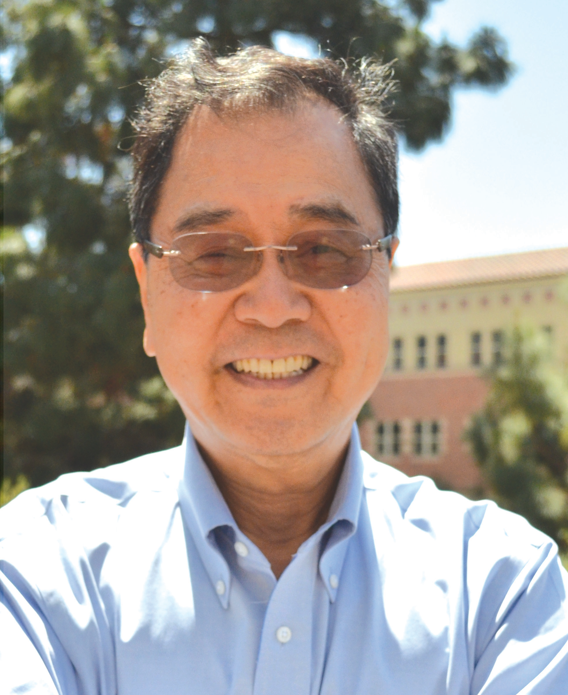 Prof. Kang Wang
Prof. Kang Wang (Univ. of California Los Angeles) will collaborate with Ching-Tzu Chen of IBM to realize antiferromagnetic exchange bias spin-orbit torque memory for Theme 4. He will also study physical phenomena related to spin-orbit coupling (such as the quantum anomalous Hall effect and spin-orbit torque) with an eye toward practical applications for topological insulators and transition metals.
Prof. Wang is no stranger to SRC research. He has collaborated with C-SPIN PIs Christian Binek and Jian-Ping Wang, and he directed the Functional Engineered Nano Architectonics (FENA) center for FCRP (STARnet’s predecessor) 2003-13.
Prof. Wang is currently the Raytheon Chair Professor of Physical Science and the primary investigator of UCLA’s Device Research Laboratory. He received his PhD from MIT in 1970, taught at MIT 1970-72, worked for General Electric Corporate Research 1972-79, and has been a member of the UCLA Electrical Engineering faculty since 1979.
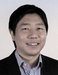 Prof. Tony Low
Prof. Tony Low (Univ. of Minnesota) will collaborate with Jian-Ping Wang to develop an atomistic simulation tool for studying MTJ devices in which the oxide layer is a 2D oxide material and Heusler alloys as magnetic contacts. This work is part of Themes 1, 2, and 4.
Before joining the Center, Prof. Low collaborated with C-SPIN PIs Steve Koester and Mo Li on a variety of projects. He has worked extensively in academia (Cornell and Yale) and industry (IBM) since receiving his PhD from the National University of Singapore in 2008. Since 2014, he has been an Assistant Professor of Electrical and Computer Engineering at the University of Minnesota.
Student and Post-Doc Profiles
 Danielle Reifsnyder Hickey
Danielle Reifsnyder Hickey
Postdoc at the University of Minnesota
I'm currently working on analytical electron microscopy research in the laboratory of Prof. Andre Mkhoyan for Theme 2. I am working to understand the atomic-scale structure and composition of heterostructured materials such as topological insulators and magnetic tunnel junctions. In both cases, the controlled growth of multiple layers of dissimilar materials is critical to making devices work, and so the interfaces must be well understood. The goal is to understand emerging materials, how they grow, and the structures they form when incorporated into devices.
I have also studied inorganic nanocrystals for energy applications, as well as batteries for implantable medical devices. My work has ranged from chemical synthesis and self-assembly to numerous types of material characterization and has resulted in several publications. Related to my C-SPIN work, specifically, two papers have been published to date, and several others either have been submitted or are in preparation.
Researching nanostructures caused me to realize that although bulk probes of structures can provide important information, some questions can only be answered by understanding local atomic configurations. Recent developments in aberration-corrected transmission electron microscopy have opened the door for directly imaging materials at that level. At the University of Minnesota, I have access to fantastic instrumentation and expertise, which makes it possible to make discoveries at an exciting frontier in materials science and engineering.
I hope to continue to contribute to the atomic-resolution understanding of complex materials. I am especially interested in expanding the knowledge of materials with electronics- and energy-based applications.
 Salinporn Kittiwatanakul
Salinporn Kittiwatanakul
Postdoc at the University of Virginia
I am currently using a novel technique, Reactive Bias Target Ion Beam Deposition, to develop high-quality Cr2O3 thin film with reduced leakage and smooth surface to be used as an insulator for voltage controlled magnetoelectric switching in p-MTJs. These thin films could improve the power consumption and reliability of spin-based systems. I’m also working on integrating metal-insulator oxides such as NbO2 and VO2 into MTJ devices and to modulate the magnetic properties of MTJ free layers using the MIT of the oxides. My work, which is overseen by Jiwei Lu, falls under Themes 1 and 4.
I have also worked as a material developer (of superconductors, magnetics, and oxides) and as a device structure designer/mask writer for lithography. Specific projects include developing a Spin Torque Nano Oscillator, developing Josephson Magnetic Random Access Memory (JMRAM) to be used in superconducting supercomputers, and studying metal-insulator transition in strongly correlated oxides for ultra-fast, low-power optical and electronic device applications. I have 18 publications, most of which are related to my work on oxide thin films.
I knew I wanted to be an experimental physicist at age 18. I was picked as one of the Thai representatives to participate in the International Physics Olympiad in 2003, and then became more and more interested in condensed matter physics, applied physics, material sciences, and engineering. I have always been excited about new electronic technologies, computers, and gadgets. I’m glad to be part of a scientific and engineering community that puts a lot of work and effort into making better, more efficient, and more advanced technologies (especially spin-based systems!).
I hope to be involved with both industrial and academic research in my future career, especially in the fields of spintronics and magnetic and oxide materials for low-power device applications. I realize how industry drives a lot of academic inquiry and how the academic world provides skilled scientists and engineers to the industry. No matter where I end up, I hope to expand my vision and experience and help improve the science and technology that will drive the future economy.
