

June 2017 Newsletter: Volume 4, Issue 2
A Message From the Director, Jian-Ping Wang
Welcome everyone, to the C-SPIN Quarterly Newsletter. C-SPIN is in its fifth and final year. I am very pleased with the many exciting results, outstanding publications, and crucial patent applications in the past 4+ years. Many of the “unexpected” outcomes arose from team efforts across multiple universities, which shows that the cross-disciplinary, multi-institutional vision of C-SPIN really does make the whole greater than the sum of its parts – and, based on SCI citations and the number of invited talks at major conferences, something that is essential for future spintronics research.
I am also very pleased with the connections that PIs, post-docs, and graduate students have made with our sponsors. We won’t know final numbers for a few months, but I think we’ll all be pleased with the number of C-SPIN graduates who have been employed by our sponsors. Some of our students and postdoctoral fellows have become professors, which means that C-SPIN ideas will continue to be developed in academia.
Finally, I am highly pleased that original C-SPIN research has developed into many other research programs that involve our PIs, including some recent DARPA and DoD MURI programs. Congratulations to those PIs, and thanks to our sponsors for their ongoing support, vision, and patience.
For this issue, I asked Mike Lotti to chronicle Theme 2, the spin channel and interfaces theme. Roland Kawakami and Paul Crowell have done an excellent job to coordinating a world-leading unique research theme that resulted in many new and exciting discoveries in the past four years.
We are really happy to see Marie Rahne back in the office after the birth of her daughter in January. Thanks to Mike and Marie again for preparing this issue of the newsletter.
Looking Back, Looking Ahead: Theme 2
All-spin logic is an incredibly promising advance that will revolutionize computing technology. Or perhaps, all-spin logic is a pipe dream. Or maybe it’s somewhere in between – which is another way of saying that the pursuit of all-spin logic will likely introduce important new technology to the world. Such a conviction has been at the heart of Theme 2 from the beginning.
All-spin logic – and other real and speculative spintronic technology – relies on ultra-low energy transport of spin from one place to another. In other words, it relies on an efficient spin channel. Back in 2012, when the original C-SPIN proposal was being written, only basic demonstrations of spin transport had occurred, and nearly all of what was recorded was not well-understood. Unlike spin-based memory, which relied on technology that had actually been developed into devices (like MTJs), all-spin logic research was almost exclusively at the “fundamental science” or “materials development” phase. No scalable materials had been developed, and no devices had been made or tested. In fact, most known spin channel materials were considered “exotic” and only worked below room temperature.
That’s why Jian-Ping Wang, along with Paul Crowell and Roland Kawakami, thought that Spin Channels deserved an entire Theme in the STARnet proposal. This would corral a variety of resources – basic materials research and fabrication, spectroscopy, interface engineering, theoretical modeling – toward the goal of developing viable spin channels at room temperature and, possibly, actual devices for testing. In the original proposal, they focused on four promising spin channel materials: 1) Two-dimensional materials, such as MoS2 and graphene. Graphene was the best-known and best-characterized material for spin channels. Moreover, it was known to function as a spin channel at room temperature with little energy input. Transition metal dichalogenides (TMDs) such as MoS2 had promising opto-electronic properties but had never been demonstrated as spin channels 2) BN on graphene. Hexagonal BN was known as a stable compound at high temperatures that could function as a tunnel barrier. 3) Topological insulators, which were just beginning to be known as potential spintronic devices. Of particular interest was Bi2Se3. 4) GaAs, which is a well-known semiconductor with outstanding electronic properties.
Theme 2 accomplishments: the first 2.5 years
The first 2.5 years of Theme 2 produced some interesting and even surprising results. Advances in graphene were highlights, even if predictable. Led by Steve Koester, C-SPIN scientists developed new, efficient ways to deposit graphene, while Roland Kawakami led the effort to test magnet-graphene interfaces. They recorded some of the first magnet-graphene spin transfer at room temperature in graphene deposited by chemical vapor deposition and were able to analyze the interfaces for a better theoretical understanding of spin properties. These efforts proved that graphene was, indeed, a spin channel that warranted further development.
Unfortunately, GaAs proved to be an inadequate spin channel material. C-SPIN investigators demonstrated GaAs spin operation at room temperature, but integration with other spintronic materials deposited by sputtering proved difficult.
The promise of MoS2 made C-SPIN researchers test and articulate some of the physics behind its properties. This suggested that TMDs, which had only been developed since 2010, should be further investigated. In general, they could be made into 2D nanosheets and had promising electric, optical, and spintronic properties.
Perhaps the biggest Theme 2 surprise in the first two years of the Center was the development of functional – that is, capable of spin transfer torque and spin pumping – topological insulators at room temperature. A paper in Nano Letters symbolized the promise of topological insulators for computing applications and led Jian-Ping Wang, Nitin Samarth, and Roland Kawakami to begin talking about a possible seminar or workshop on topological insulators.
Theme 2 accomplishments: the next 2 years
The realignment in 2015 led to three big changes for Theme 2:
- TMD and GaAs research was dropped. Both were still too much in the “basic science” stage of research to be promising candidates for spintronic devices within the next 5-10 years.
- More resources were devoted to studying and developing topological insulators. This included an agreement to host a C-SPIN-sponsored, first-ever workshop on topological insulators.
- Theme 3 was absorbed under Theme 2’s umbrella. The retirement of Bill Butler (Theme 3 Leader) and the untimely death of Oleg Mryasov (Theme 3 PI), along with the successful completion of some of Theme 3’s goals, made it simpler for the C-SPIN to administer four full Themes.
These changes did not affect the Center’s dedication to developing graphene. In the past two years, Theme 2 has demonstrated that SrO works as a tunnel barrier to control a graphene-magnet interface and a record-breaking (by a factor of 4) spin accumulation of 2.0 mV. In particular, SrO has enabled a new generation of robust graphene-based spintronic devices. Furthermore, Theme 2 demonstrated the longest room temperature spin lifetimes for hexagonal BN tunnel barriers on graphene. Given that these demonstrations happened at room temperature and that C-SPIN researchers (and others) continue to improve deposition techniques, graphene is still a possible foundation for future all-spin logic and memory-logic systems. Much remains to be done: graphene spin injection efficiency is typically less than 20% and needs improvement, and several theoretical puzzles remain about graphene interfaces and, indeed, graphene itself.
The first-ever Topological Insulator Workshop held at the University of Minnesota in August 2016 was a clear sign that C-SPIN – which sponsored and hosted the event – was indeed at an important forefront of spintronics research. Two topological insulators on YIG – Bi2Se3 and (BiSb)2Te3 – showed dramatic spin pumping results at room temperature. Building on this, Jian-Ping Wang recently demonstrated two-terminal switching in two papers and a patent -- something that industry sponsors are very interested in, especially since such switches can potentially serve in logic, memory, and storage applications.
After C-SPIN
Much remains to be done before C-SPIN’s work makes its way into everyday computing technology – better graphene and more basic science research on topological insulators, TMDs, and GaAs, for example. But the spin channels developed by C-SPIN in the last four years, along with the materials and device research behind them, will likely be important foundations for the spintronic computing of the future.
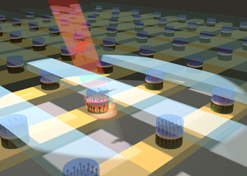
Flipping a Magnetic Memory Cell with a Light Pulse
C-SPIN researchers have created a magnetic tunnel junction (MTJ) that can be switched by a pulse of light lasting one trillionth of a second, setting a speed record. The magnetic tunnel junction is a device critical to information technology with the termination of Moore’s law, a principle that has ruled the microelectronics industry for five decades.
This advancement holds promise for the development of new, optically controlled, ultrafast magnetic devices collectively called spintronics (electronics that combine optical and magnetic nanotechnologies). These devices could lead to innovations in the storage, processing, and communication of information in the coming decade. An example of such innovation would be the development of a system that like the human brain, can both store and analyze a large amount of data simultaneously.
The details of the device and the tests conducted on it are reported in the paper “All-optical switching of magnetic tunnel junctions with single sub-picosecond laser pulses,” published on Feb. 28 in the journal Physical Review Applied.
Typically, the MTJ has a sandwich-like structure comprising two layers of magnetic materials with an insulating layer, called barrier, in the middle. Information is written on the magnetic material by reversing the magnetization of one of the layers. This reversing process often involves spiral motion in the spinning electrons, called spin processing. However, there are is a limitation on how fast the spin processing can be; the brakes are applied at roughly 1.6GHz, a current speed record that is much slower than silicon transistors. To enable faster writing speeds, the limitations on speed have to be overcome.
With the invention of a new MTJ by scientists at the University’s Department of Electrical and Computer Engineering, there is now a way to speed up things. Inspired by the 2007 discovery by Dutch and Japanese scientists that the magnetization of an alloy of gadolinium (Gd), a rare earth element, iron (Fe), and cobalt (Co) could be switched using light pulses, our scientists used the alloy to replace the upper magnetic layer of a conventional MTJ. Another modification they made to the device was to use a transparent electrical material called indium tin oxide for the electrode to allow light to pass through it. These layers are stacked into a pillar with a diameter of 10µm, which is only one tenth the diameter of a typical human hair.
To test, scientists sent laser pulses to the modified device using a low-cost laser based on optical fibers that emits ultrashort pulses of infrared light. The pulses are sent one in every microsecond (a microsecond is one millionth of a second). Every time a pulse hit the MTJ pillar, the scientists observed a jump in the voltage on the device. The change in voltage confirms that the resistance of the MTJ sandwich changes each time the magnetization of the GdFeCo layer is switched. Because each laser pulse lasts less than 1 picosecond (a millionth of a microsecond), the device is capable of receiving data at a rate of 1 terabit per second!
For Prof. Mo Li, one of the lead scientists, the outcome holds exciting prospects. “Our result establishes a new means of communication between fiber optics and magnetic devices. While fiber optics afford ultra-high data rate, magnetic devices can store data in a non-volatile way with high density.”
According to C-SPIN director, Prof. Jian-Ping Wang, also a lead scientist on the project, “The results offer a path towards a new category of optical spintronic devices that have the potential to address bandwidth limit and scaling challenges for future intelligent systems. These systems could use spin devices as neurons and synapses to perform computing and storage functions just like the brain, while using light to communicate the information.”
The ultimate goal for this research team is to shrink the size of the MTJ to less than 100 nanometers and reduce the required optical energy. To this end, the team is continuing its research, and is currently engaged in optimizing the material and structure of the device, and working on integrating it with nanophotonics.
Save the Date for the 2017 Annual Review
The 2017 C-SPIN Annual Review will be held in Minneapolis on September 27th and 28th. Registration will be announced in the coming weeks. We are looking forward to seeing you in Minneapolis once again!
Student and Post-Doc Profiles
Gordon Stecklein, PhD Candidate, University of Minnesota
 Gordon Stecklein
I am working on spin transport through graphene/ferromagnet interfaces, which is a project in Theme 2. The goal is to understand how the materials and electrical resistance of these interfaces affect our ability to both inject spins from a ferromagnet into graphene and absorb spins from graphene into a ferromagnet. Nonlocal graphene spin valves are an ideal system for electrostatically gating spin currents, which could be useful for switching magnetizations by spin-transfer torque and spin-based neuromorphic computing.
I am also interested in graphene grown by chemical vapor deposition. Historically, this growth method, which produces larger area graphene than exfoliated techniques, results in films with reduced mobility. I have four publications to my credit and two underway with fellow C-SPIN researchers Walid Amamou and Yoska Anugrah.
My experience working for an electric utility on the adoption of solar, wind, and energy storage technologies made me wish for a better fundamental understanding of advanced materials, which led me to research in experimental condensed matter physics. I appreciate working on every step of a project from fabrication through modeling.
I expect to graduate near the end of this summer and am looking at teaching and research jobs in the greater Los Angeles area. While I enjoy teaching at the undergraduate level, I am also interested in applying the techniques I have learned in graduate school to answer a broad range of questions – including those in the energy sector – that are both societally impactful and technologically complicated.
Walid Amamou, Postdoctoral Researcher, The Ohio State University
 Walid Amamou
I am working on achieving non-local magnetization switching of a nanomagnet deposited on graphene. The role of the graphene here is to carry spin current to the nanomagnet in order to switch its magnetization by spin transfer torque (STT). Graphene is an excellent spin conductor with a spin diffusion length up to 30 μm and is therefore an ideal platform for achieving magnetization switching. In collaboration with the Crowell and Koester groups, we discovered that the spin current is significantly reduced and relaxed at the nanomagnet/graphene interface before getting absorbed to the bulk of the nanomagnet and converted to useful STT. While this might seem like a bad news for graphene, we discovered that by inserting a Cu spacer between the ferromagnet and graphene, we could strongly reduce this interfacial spin relaxation effect and observe bulk spin absorption that is essential for achieving magnetization switching. This work is in Theme 2 and is of particular importance for achieving viable All-Spin Logic devices which heavily rely on non-local magnetization switching.
I have also been working on magnetic proximity effect using the ferrimagnetic insulator CoFe2O4. We successfully demonstrated the presence of magnetic proximity in Pt using CoFe2O4 for the first time. This effect can be extended to 2D materials such as graphene, which could allow the realization of future spin FET. Overall, I have two first author publications and 5 co-author publications. We are also planning to submit two more publications very soon for which I will be first author.
I knew from the beginning that I wanted to study physics but I was not sure which area to focus on. During my undergrad and master’s studies in France, I had the chance to explore multiple branches of experimental physics, but was immediately attracted by condensed matter physics. During my master’s studies, I had the opportunity to do an internship at the University of Tokyo, and that’s where I discovered the fascinating field of spintronics.
I hope to be able to contribute to the development of spintronic devices that can be used in our everyday lives. I spent most of my career so far in academia and would like to transition to industry where I can apply my knowledge and skills to commercial products. Starting June 2017, I will begin my new employment at Intel Corporation and embark on a new journey in the tech industry.
