January 2017 Newsletter: Volume 4, Issue 1
A Message from the Director, Jian-Ping Wang
First of all, congratulations to Caroline Ross and Geoff Beach for their new article in Nature Materials on the first instance of current-induced switching in a magnetic insulator. It’s a truly exciting result. See our news feed for more details.
More congratulations are due to Sachin Sapatnekar, who was recently named a 2016 fellow of the Association for Computing Machinery, and Steve Koester, who was recently named a fellow of IEEE. As someone who has seen their consistently excellent work in and out of C-SPIN, I am not surprised by these honors.
Second, please note that Marie Rahne, our hard-working Center Manager, will be on maternity leave for the next three months. Most of Marie’s duties will be filled by C-SPIN executive assistant Sylvia Hill. You can contact Mike Lotti about news and other communications items.
Third, in the final year of C-SPIN, I thought it would be good to both look back on our progress and look ahead – as best we can – to see how our work may bear fruit in industry and academia. So I instructed Mike Lotti, our communications coordinator, to write five articles for the final three newsletters, with hopes that we can have something like a history of the Center by the time of our final Annual Review in September. Because of the limited space and time, he only could pick up some highlights – I’ll trust you to dig out more from previous C-SPIN newsletters. In this issue, Lotti recounts the beginning of C-SPIN (which he was a part of) and the interesting journey of Theme 1.
Looking Back, Looking Ahead: The Birth of C-SPIN
Major scientific research centers don’t happen by accident, and they don’t happen easily. They require vision, administrative and organizational expertise, plenty of institutional support, and, of course, a huge amount of high-level scientific expertise. On top of all that, they require cooperation and a lot of money – as in tens of millions of dollars.
To understand how C-SPIN came to be, it’s best to start with the vision and the money. And the vision starts with Jian-Ping Wang and his team.
Growth of Non-volatile Spintronics Research
Magnetic semiconductors have been the mainstream for spintronics research and its application for logic since 1990. Unfortunately, its operation demands low temperatures and so couldn’t support CPUs in PCs, laptops or mobile devices. At a 2004 symposium organized by the University of Alabama on magnetic tunnel junctions (MTJs), Jian-Ping Wang gave a talk on the potential advantages of non-volatile spintronic logic and presented the world’s first experimental demonstration of an MTJ array. Using MTJs for read sensors in hard disk drives and MRAM was well underway by that time, but Wang felt like he was the only one to apply the same principles to the other main parts of a computer. “I pictured people in resource-poor or resource-unstable settings still being able to use computers and maybe even power them up with simple solar cells,” Wang remembers. “I also tried to articulate all the advantages of non-volatile systems, including non-volatile memory.”
Wang’s talk was, in many ways, the natural product of good training combined with a restless mind. Before joining the University of Minnesota, he taught about and developed magnetic materials for data storage in Singapore for seven years. “I developed more and more familiarity with the field, which led me to keep thinking, ‘There’s so much more we can do with magnetic materials. Why aren’t we doing it?’” says Wang. When he joined the University of Minnesota faculty in 2002 – a “huge decision,” he says, because of his family and his career trajectory – he felt more free to “think big” and “think outside the box.”
The result of Wang’s 2004 talk in Alabama was a publication (“A Spintronics Full Adder for Magnetic CPU”, IEEE ELECTRON DEVICE LETTERS, 26, 360 (2005)) – but not much else. The alarm bells about the “need to beyond CMOS” weren’t very loud at that point, and Wang notes that nothing beyond GMR was well-known: nobody had made a MTJ logic gate, and very little was known about efficient magnetic materials, much less interfaces and interconnects. Spintronics for “beyond CMOS” computing and memory was not an established discipline, and most spintronics research was siloed or, at most, confined to projects with two or three PIs.
Fast forward to 2010 and a much-changed world of computing research. The need for “beyond CMOS” materials, devices, and architectures was a common refrain. DARPA and NSF began funding research into alternatives to CMOS, and the Semiconductor Research Corporation (SRC) signaled that it would invest heavily in “beyond CMOS” research centers in the 2013 round of funding. And spintronics had grown: dozens of new materials had been made and characterized, the advantages of perpendicular magnetic anisotropy had been discovered, and there were several new ways to control and convey spin.
In other words, spintronics was now a mainstream pursuit (especially for non-volatile memory applications), and it was recognized that spintronic computing held the most promise for ultra-low power neuromorphic computing and future artificial intelligence, even if the technologies were admittedly years from development. There was also a strong sense that new measurement and nanofabrication techniques would lead to discoveries that could radically accelerate spintronics development. On top of that, dozens of researchers from industry and academia had collaborated on hundreds of projects, and publications were increasing by the year.
But even in 2010, there was very little large-scale, coordinated spintronics research in the U.S. That required money, which brings us to SRC and its push to rapidly advance “beyond-CMOS” research.
SRC: A New Possibility for Spintronics Research
SRC began in 1982 as way to fund “pre-competitive” computing technology research. Within 10 years, it had pioneered the now-famous TECHCON conferences, sponsored hundreds of research collaborations, welcomed a half-dozen federal agencies into its ranks, and published the groundbreaking National Technology Roadmap Standards (NTRS). In 1997, it established the Focus Center Research Program (FCRP) to accelerate innovative, multi-university research in semiconductor technology with a horizon of eight-plus years through multi-university centers.
In 2012, FCRP became STARnet. Led by Intel’s Gilroy Vandentop, its mission was big but simple: continue FCRP’s forward-looking sponsorship, but through six new research centers starting in 2013. More specifically, STARnet aimed to drive “beyond-CMOS” research that exceeded even the NTRS horizon. Even more specifically, STARnet’s call for proposals noted the promise of spin-based materials for traditional, quantum, and novel computing architectures. And STARnet was backing up its commitment, promising $25-30 million per five-year research center.
The Papers: Creating C-SPIN
Jian-Ping Wang realized that this was, perhaps, a once-in-a-lifetime opportunity to organize the U.S. spintronics research community and build a vertically integrated center for advanced spintronic research. With University of Minnesota colleagues Paul Crowell, Steven Koester, Chris Kim and other researchers, Wang compiled a six-page white paper articulating a Center with the five research themes we have today. After reviewing it, STARnet asked that he combine forces with a team behind another white paper and submit a full proposal. And the rest, as they say, is history.
Except that it wasn’t easy history to make. Wang and his leadership team spent three months recruiting researchers, negotiating contracts, coordinating drafts, and making one voice out of many. The end result was massive: 50 carefully organized pages of a research proposal, 40 pages of references and biosketches, and over 200 pages of contracts, budgets, budget justifications, and intellectual property agreements. STARnet required a paper submission, so on September 13, 2012 – one day before the proposal was due at STARnet – Wang, Koester, Mike Lotti, and a few graduate students dedicated four or five hours to carefully assembling five (or maybe six) copies of the proposal. We counted pages, re-counted pages, checked and double-checked pages, and made more than a few last-minute edits and substitutions.
About five weeks later, STARnet informed Wang that C-SPIN would become a reality. Wang quickly arranged for Marie Rahne, who was the coordinator for the Fine Theoretical Physics Institute on the University of Minnesota campus, to be Center Manager.
And the rest is, indeed, history, even ongoing history. And you can read more about that in the Theme-based articles that will follow.
Looking Back, Looking Ahead: Theme 1
“Lots of promising research, not much organization to fulfill that promise.” That’s Jian-Ping Wang’s characterization of spintronics research prior to C-SPIN. Regarding Theme 1, that meant that a few things were well-known, but it was unclear if (and when) substantial breakthroughs would move the field toward viable spintronic memory and logic devices.
Everyone knew that perpendicular magnetic anisotropy (PMA) materials were essential to robust spintronic computing, for example, but only a few good PMA materials had been characterized by 2012, and no one knew how they would perform when interfacing with other materials – or even if they could survive high-temperature annealing and then function well at room temperature.
Another example: it was clear that a device like a magnetic tunnel junction (MTJ) would be necessary, but no one knew how such devices would be used (replacements for FETs? translators of spin information to CMOS systems?) or if they could be small enough to compete with CMOS devices.
The Plan
For C-SPIN leadership, the way to address these (and many other) issues was simple: create an infrastructure that integrated the work of fabricators, experimentalists, measurement experts, and theoreticians so that hundreds of samples, interfaces, and proto-devices could be developed and characterized. More specifically, C-SPIN proposed to:
- Develop and characterize dozens (maybe hundreds) of new PMA materials
- Develop new ways of depositing magnetic oxides and magneto-electric materials
- Develop new techniques for nanopatterning magnetic structures, especially MTJs
- Fabricate spintronic materials and devices that could be switched with ultra-low voltage
Implicit in the initial C-SPIN grant proposal was the expectation of surprises: some promising materials and devices wouldn’t work out, and some that were not-so-promising (or even unknown) would turn out to be better than anyone could have imagined.
Theme 1 Accomplishments
The Theme 1 team – led by Chia-Ling Chien and Caroline Ross – has 13 PIs, seven cross-Theme PIs, and dozens of graduate students and post docs. It has basically accomplished what it promised four-and-a-half years ago. Dozens of new materials have been fabricated and characterized, along with dozens of material combinations and proto-devices. Nanopatterning procedures have improved, resulting in smaller and smaller proto-devices, some with diameters less than 20 nm. Materials and proto-devices have been switched with ultra-low voltage, including some antiferromagnetic materials. Jian-Ping Wang highlights six specific accomplishments:
- Two new types of magnetic insulators with bulk perpendicular anisotropy have been developed and demonstrated with spin Hall switching.
- Perpendicular super lattice Heusler alloy materials, which were predicted by Bill Butler, have been fabricated for the first time.
- Magnetic tunnel junctions with FePd synthetic antiferromagnetic structures have been demonstrated for the first time and proven to be excellent for 3D logic and memory.
- Voltage-controlled exchange bias Cr2O3 stacks have been demonstrated with higher Neel temperature with B doping, and an ultra-thin Cr2O3 film down to 10 nm without leakage was successfully demonstrated.
- Voltage-controlled magnetism for nanoscale magnetic devices has been demonstrated several times.
- Spin damping is much better understood, both in terms of measuring it and understanding its correlation with atomic structure. This has led (and will lead) to more rapid development of spintronic materials and devices.
Looking Ahead
Of course, Theme 1 research is not over. Over the next seven months, Theme 1 PIs hope to further demonstrate 1) A voltage-controlled exchange bias switchable memory cell; 2) Electrical field induced switching in MTJs with bulk PMA; 3) Magnetoelectrically switching Heusler alloy structures; and 4) External field free switching of a PMA structure using the spin Hall effect.
It’s safe to say that Theme 1 has fulfilled STARnet’s original goal of producing research and technologies that will fulfill needs on an 8-year time frame. All the highlights noted above – along with many others – are ready for accelerated development in academia and industry and could be in memory, logic, quantum computing, and other applications by 2020.
In other words, Theme 1’s integrated structure has quietly opened the floodgates for future spintronic computing and memory.
C-SPIN Associate Director, Prof. Steven Koester Named IEEE Fellow
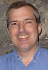
 Steve Koester
University of Minnesota Prof. Steven Koester has been named an IEEE Fellow effective January 2017. He is cited by the IEEE for “contributions to group-IV electronic and photonic devices.” Prof. Koester’s research focuses on novel electronic, photonic and sensing device concepts with an emphasis on graphene and other 2D materials. He has authored or co-authored over 200 technical publications, conference presentations, and book chapters, and holds 65 United States patents. Prof. Koester is also an associate editor for IEEE Electron Device Letters.
Steven Koester earned his doctoral degree in 1995 from the University of California, Santa Barbara. From 1997 to 2010 he was a research staff member at the IBM T. J. Watson Research Center and performed research on a variety of electronic and optoelectronic devices, with an emphasis on those utilizing the Si/SiGe material system. From 2006-2010 he served as manager of Exploratory Technology at IBM Research where his team investigated advanced devices and integration concepts for use in future generations of microprocessor technology. Since 2010, he has been a Professor with the Department Electrical and Computer Engineering at the University of Minnesota.
The grade of Fellow, the highest membership grade, is conferred by the IEEE Board of Directors on individuals with an outstanding record of accomplishments in an IEEE field of interest. Fewer than one-tenth of one percent of the total number of voting members are elevated as Fellows. The grade is recognized by the technical community as a prestigious honor and an important career achievement.
C-SPIN PI, Prof. Sachin Sapatnekar Named ACM Fellow
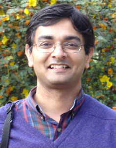
 Sachin Sapatnekar
The Association for Computing Machinery has named Prof. Sachin Sapatnekar as one of its 2016 ACM Fellows for “contributions to the enhancement of performance and reliability in integrated circuits.” Prof. Sapatnekar’s research focuses on computer-aided design (CAD) of VLSI systems. Some of the specific problems that his research team have worked on recently include spintronics-based design, thermal analysis, reliability, timing analysis and optimization, power grid analysis, and 3D integration.
Sachin Sapatnekar earned his doctoral degree in 1992 from the University of Illinois at Urbana-Champaign. From 1992 to 1997, he was an Assistant Professor in the Department of Electrical and Computer Engineering at Iowa State University. He joined the Department of Electrical and Computer Engineering at the University of Minnesota in 1997, and holds the Robert and Marjorie Henle Chair and the Distinguished McKnight University Professorship. He has served on the editorial boards of several IEEE journals, and also as Editor-in-Chief of the IEEE Transactions on CAD. He has been technical program chair and general chair for several conferences. These include the Design Automation Conference (DAC), and the International Symposium on Physical Design (ISPD). He is a recipient of the NSF Career Award, the SRC Technical Excellence Award, the SIA University Researcher Award, and several Best Paper Awards at the DAC and other conferences. Most recently, he received the ICCAD Ten-Year Retrospective Most Influential Paper Award for the second time. He is also a Fellow of IEEE.
The Fellows program was established by the ACM in 1993 to recognize the professional, technical and leadership-based contributions of its outstanding members. The number of members recognized as Fellows cannot exceed one percent of the number of ACM professional members. The 2016 Fellows have been recognized for contributions in areas that impact our work and daily life. These include cloud computing, computer security, data science, Internet routing and security, large-scale distributed computing, mobile computing, spoken-language processing and theoretical computer science.
Student and Post-Doc Profiles
Andy Quindeau, Postdoctoral Researcher with Prof. Caroline Ross at MIT
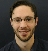
 Andy Quindeau
My work involves the fabrication and characterization of perpendicularly magnetized ferromagnetic insulators (here Tm3Fe5O12) that are notoriously difficult to synthesize (Theme 1). I collaborate with C-SPIN affiliates to produce spintronic devices that use spin currents to switch these ferromagnets. Ultimately, the implementation of perpendicular ferromagnetic insulators will be better than metallic devices in terms of switching efficiency and could potentially lead to dissipationless current transport in conjunction with topological insulators.
I am also working on the ferromagnetic resonance characterization of thin films in order to quantify important properties like ferromagnetic damping as a function of temperature. My research as a C-SPIN affiliate over the last year has led to two publications: the first one involves the magnetic characterization of the perpendicular magnetic insulator thulium iron garnet, and the second one describes the first demonstration of a ferromagnetic insulator switched by a pure spin current.
My fascination for materials science arose from the fact that material properties can vary dramatically just by a change in crystal structure. Carbon, for example, possesses very good conducting properties as graphite but is one of the best insulators when a diamond. As I got more experience in the field of low dimensional electronic systems, multiferroics, and (especially) magnetism, I developed a strong desire to understand and combine different materials and properties, which is perfectly exemplified throughout the field of spintronics.
I want to continue engineering-oriented research that is directed toward real device applications. I highly value my experience of fundamental research on 2-dimensional electron systems, but I believe that I am most productive in a goal-driven research/engineering environment, where a deep fundamental and intuitive understanding of a variety of physical phenomena plays a crucial role – but not the only role. This is why I am most interested in a career devoted to hands-on, state-of-the-art technology innovation in the tech industry.
James Kally, Ph.D. Candidate with Prof. Nitin Samarth at Penn State University
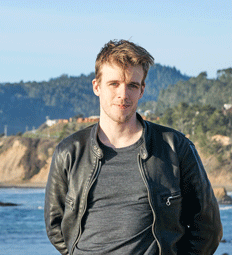
 James Kally
I am currently working within Theme 2 to utilize topological insulators as spin injectors and spin channels. Topological insulators have the exciting property of conducting surface states where the spin of the electron is “locked” with its momentum. Since the direction of the current defines the electron’s spin orientation in a topological insulator, they could be very efficient for switching a magnet. In particular, I work with topological insulators Bi2Se3 and (Bi,Sb)2Te3, which I grow by molecular beam epitaxy on a variety of substrates in Prof. Nitin Samarth’s lab at Penn State.
I am also working with other C-SPIN groups on 1) interfacing topological insulators with ferromagnetic insulators and graphene, and 2) growing topological insulator thin films for magnetic junctions. I have various publications in progress as a first author and as a contributing author; they all indicate that topological insulators could be efficient for spin devices. As an undergraduate, I studied the opening of a gap in the energy states in NdNiO3 by electron tunneling as the material undergoes a metal-to-insulator transition.
I became involved in research through a summer internship in Prof. Jim Allen’s lab at UCSB before starting a bachelor of science program in physics at UCSB. From there it has been one fascinating project after another at UCSB, Trinity College Dublin, HRL Laboratories, and Penn State. It is so rewarding after sometimes struggling for months to finally get a material to grow properly or see exciting data. One defining moment in my second year at UCSB: I was with my advisor, his post-doc, and a scientist from Intel who was working with SRC. They were discussing an idea for magnetic logic using frustrated magnetism in a triangle pattern. That moment felt like we were planning the future of electronics. Working in spintronics leads to so many of these moments – you feel like you can create something impactful.
I am planning on moving to R&D in industry after I graduate. I want to continue developing materials for device applications. I am interested to see what advances will be incorporated in future microprocessors, and I want to be a part of those advances.


