
Month Year Newsletter: Volume 2, Issue 3
A Message From the Director, Jian-Ping Wang
Welcome everyone to the 7th C-SPIN Quarterly Newsletter. C-SPIN has finished the 2.5 year re-alignment process. I would like to thank the STARnet program directors and SAB members for their insight into how to make C-SPIN more focused and stronger through 2018. I also thank all C-SPIN PIs for their great efforts during the internal review in May and their understanding as we devised the 2.5 year re-alignment plan. The first article in this newsletter is my summary of C-SPIN’s direction for the next 2.5 years.
C-SPIN has been challenged from day one to answer critical fundamental questions related to spintronic materials, devices and systems for logic and memory applications. More specifically, we have striven to understand, design, and synthesize high-quality spintronic materials that go beyond today’s available candidates including commercialized CoFeB. Our recent international workshop on Heusler alloys – perhaps the first and only such workshop of its kind – was a direct outgrowth of that effort. I would like to thank Marie Rahne for her smooth handling of all the logistics for this successful workshop. You will see a summary of the workshop in this newsletter.
Lastly, a big congratulations to Prof. Kaushik Roy on receiving the prestigious 2015 DARPA Fellowship based on his pioneering effort on spin-based neuromorphic computing research.
Midway Through the Journey
By Jian-Ping Wang, C-SPIN Director
“You know, C-SPIN isn’t just at the frontiers of spintronic science and technology. It’s creating new frontiers.”
That’s what Mike Lotti, our communications coordinator, recently said to me as we were discussing this newsletter. He’s right, and his words helped me put the C-SPIN 2.5-year Center realignment in context.
In some ways, Mike stated the obvious. But it’s easy to forget the obvious amidst all of the emails, phone calls, meetings, reports, graduate seminars, and other tasks that fill our days. As a veteran of spintronics research, the most exciting part of my work is identifying and solving problems while pursuing new knowledge, and the first 2.5 years of C-SPIN have made me feel right at home.
I’m still excited, for example, by Geoff Beach and Weigang Wang’s discovery and demonstration of electrically controlled magnetism, the birth of the topological insulator spintronics with the early involvement from Nitin Samarth and his collaborators, the prediction of a family of perpendicular Heusler alloys by Bill Butler, the nurturing of antiferromagnetic spintronics and the first demonstration of electrically tunable transport in one antiferromagnetic oxide by Maxim Tsoi, the benchmarking and maturing of spin-based neuromorphic computing concept by Kaushik Roy and Anand Raghunathan. Of course, I look forward to similar surprises in the next 2.5 years. And while it’s been disappointing to discover the engineering difficulties of the integration of CPP-GMR with ultra-thin heavily doped semiconductor layer, the fundamental challenges of using TMD and III-V materials for spin channels, and the ambiguous goal of tackling spin-based processor design in the early days of the center, it’s also exciting in a way. That’s life on the scientific frontier, and “disappointing” discoveries always point us in better, more promising directions.
Again: C-SPIN really is creating new frontiers. Our main goal is spintronic computing, but many other scientists in many other fields will extend our work on Heusler alloys, low damping PMA materials, and multiferroic materials. We’ve also opened up new frontiers in spintronic fabrication. It’s easy to forget that until C-SPIN, no one had even tried to fabricate a topologic insulator-based spin pumping device operating at room temperature and key components for a spin-optical based interconnect, and what we’ve learned will no doubt be applied in other fields.
And our focus on fabrication is really just starting, which brings me to C-SPIN’s realignment plan. I won’t try to explain all the details of our realignment plan, but I want to try to sketch the broad contours of the next 2.5 years at C-SPIN – which of course include room for surprises, both good and bad. If I had to summarize the next 2.5 years at C-SPIN, I’d say something like “We’re shifting our focus from full discovery mode to discovery plus feasibility demonstration,” or perhaps, “We’ll focus more on the implementation of many exciting devices and systems theories and many newly predicted materials.”
I know that it’s more complicated than that. The last 2.5 years have included device fabrication and experimentation, and the next 2.5 years will undoubtedly be full of important discoveries and theoretical work. But the overall focus has shifted. We cast our net wide in 2013, knowing that, as we established our processes for working with one another, we’d pull up a lot of useful and non-useful information. Now it’s time to take what’s useful and learn how to make substantial, directed progress toward spintronic devices that work and show promise for beating CMOS performance.
In terms of multi-Theme tasks, this means that we will be focusing on
- Developing new ways to grow promising Heusler alloys and rigorous testing of the alloys themselves
- Measuring spintronic logic and memory devices against benchmarks and testing ways to improve performance
- Emphasizing one well-benchmarked spin device concept (e.g. spin majority gate) that connects the five Themes and spurs more specific cross-Theme collaboration and concrete deliverables
On a Theme-by-Theme basis, my quick overview of the 2.5-year realignment looks like this
- Theme 1: There are too many tasks to list here, but we will generally continue the work of the first 2.5 years but with a much smaller group of materials and with more defined benchmarks.
- Theme 2: We will focus almost entirely on graphene and TI spin channels: improving the yield and performance of graphene spin valves, integrating graphene with PMA and TMD materials, and using graphene to improve topological insulators.
- Theme 3: We will grow and test perpendicular Heusler alloys for memory and logic devices and analyze interfaces of the best spintronic heterostructures.
- Theme 4: In order to design, build, and characterize new devices within the next two years, we will develop spin-optical interconnects, spin-orbit torque memory devices (especially those with RT AFM materials), and graphene directional materials.
- Theme 5: Like Theme 1, we will continue the work of the first 2.5 years but with a better, more focused set of devices and systems that have been identified as promising.
As C-SPIN Director, I’ve had a front-row seat to some exceptional science and engineering over the past 2.5 years. I am sure that I’ll be saying the same thing in 2018.
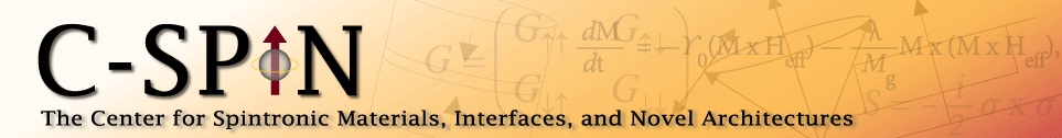
 Professor William H. Butler and C-SPIN
 Director Jian-Ping Wang
Heusler Alloys for Spintronic Devices Workshop
Sometime around 1900, an obscure German chemist noticed something unusual. Having grown up around his father’s small metalworks factory, Friedrich Heusler knew that an alloy of three non-magnetic metals shouldn’t be magnetic. But when he put copper, tin, and manganese together, the first “Heusler alloy” was born. Nearly 115 years after this discovery, over 1000 possible Heusler alloys have been identified and dozens have been fabricated and tested. These alloys are potential semiconductors, ferromagnets, antiferromagnets, superconductors, and topological insulators.
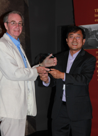
Last month, 18 top scientists from the United States, Germany, Japan and Great Britain gathered at the University of Minnesota to discuss Heusler alloys and their application to spintronic devices. Another 20 industry participants from semiconductor industry giants (such as Intel, Seagate, and Western Digital) and startups (such as Spin Transfer Tech) also participated. More than 20 C-SPIN students and postdoctoral fellows attended the workshop on site, and several C-SPIN industry associates joined the workshop online.
STARnet program executive director Gil Vandentop and DARPA STARnet program director Avram Bar-Cohen gave kickoff speeches, expressing the urgent need for new materials and the importance of the Heusler workshop to STARnet and future DARPA programs. C-SPIN director Jian-Ping Wang gave a short introduction to C-SPIN and the importance of Heusler alloy research to C-SPIN and future nanoelectronics.
The workshop began with a plenary talk by Intel researcher Ian Young, a world leader in benchmarking CMOS and beyond-CMOS devices. He primarily discussed the promise of perpendicular spintronic devices containing Heusler alloys. He also presented a benchmarking chart that positioned some perpendicular spintronic devices on par with future CMOS devices in terms of energy and delay product.
Young’s presentation was followed by 17 formal presentations covering all aspects of Heusler alloys research: William Butler (University of Alabama) presented his calculations of more than 300 Heusler alloys and their performances. More excitingly, he demonstrated his Heusler web database, which allows users to calculate Heusler alloys and their basic performances. Claudia Felser (Max Plank Institute) reviewed the Heusler alloys research and progress, and more specifically shared her recent work on perpendicular Mn2 Heusler alloy. A variety of Heusler alloy based devices and their progress (e.g. MTJ and CPP-GMR) were reported by Gunter Reiss (Bielefeld University), Koki Takanashi (Tohoku University), Kazuhiro Hono and Hiroaki Sukegawa (National Institute for Materials Science Japan), and Paul Crowell (University of Minnesota). Gautam Shine (Stanford University), Oleg Mryasov (Western Digital) and Richard James (University of Minnesota) presented their theoretical efforts on new applications for Heusler alloys. Kanta Ono (High Energy Accelerator Research Organization, Japan), Martin Jourdan (University of Mainz), Chris Leighton (University of Minnesota) and Atsufumi Hirohata (York University) all reported the characterization of Heusler alloys by different fundamental tools including neutron and synchrotron x-ray and high resolution TEM. Chris Palmstrøm (University of California, Santa Barbara) and Matthew Carey (Spin Transfer Technologies) presented their successful deposition processes to grow Heusler alloy films with desirable properties.
The personal highlight of the workshop was the special recognition of William Butler, who is newly-retired from the University of Alabama. Butler predicted the existence of giant magnetoresistance of MgO-based MTJs and has contributed more to the understanding of Heusler alloys than anyone else.
C-SPIN, Seagate, SRC, and the STARnet program teamed up to sponsor the Heusler workshop. Presentations from the workshop are available to view on the workshop webpage.
C-SPIN 2015 Annual Review
The C-SPIN 2015 Annual Review will be held at the University of Minnesota, Minneapolis September 16-17, 2015. We will use two full days for the review, beginning the program in the morning of Wednesday the 16th and wrapping up late afternoon of the 17th. The Annual Review is open to all researchers, graduate students, post-docs, SRC members, and industry sponsors. Everyone planning to attend the annual review must register.
Please visit the C-SPIN website to REGISTER. Registration closes August 16th.
The deadline for making hotel reservations is also August 16th. Please visit the C-SPIN website for more details about the review and the review agenda. Questions regarding the review can be directed to Marie L. Rahne at: cspin (AT) umn.edu
 Kaushik Roy
Kaushik Roy Named a National Security Science and Engineering Faculty Fellow
Prof. Roy of Purdue University has been named one of ten 2014 National Security Science and Engineering Faculty Fellows (NSSEFF) by the DOD Research and Engineering Enterprise. Up to $3 million of research support will be granted to each fellow for up to five years, enabling transformative research. The fellows conduct basic research in core science and engineering disciplines that underpin future DOD technology development. Prof. Roy was named fellow in the topic of Neuromorphic Computing. Read More.
Student and Post-Doc Profiles
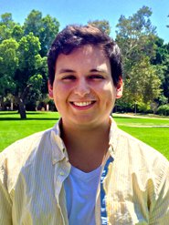 David Barroso
David Barroso
Ph.D. candidate at the University of California-Riverside
I am currently working on spin channel materials for Theme 2. My specific contribution is the synthesis via chemical vapor deposition of new transition metal dichalcogenides (TMDs) such as WSe2, MoS2(1-x)Se1-xe and MoSe2 and synthesizing these (along with other 2D materials) into lateral and vertically stacked heterostructures. I particularly focus on WSe2 because the heavy nature of the atoms involved offers maximum spin orbit interaction and ensuing spin splitting. Ultimately, I believe that in-situ integration of 2D materials into heterostructures is vital to the future of industrial semiconductors.
I have also worked on the photoresponse of TMD alloys with varying S:Se ratios, which led to a recent publication in Nano Letters. As a member of Ludwig Bartels’ group, I have contributed to other publications on MoS2 derivatives.
I am a researcher because of the encouragement Dr. Bartels gave me as an undergraduate in his lab. During that time, I found that the intersection of thin film materials and future semiconductor technology is where my interests lie. I am fascinated by the potential our films have for real devices and how 2D materials will revolutionize semiconductor technology. I love challenging myself to get to the limits of technology and physics and trying to go beyond them.
I hope to continue to contribute to the semiconductor industry as a post-doctoral researcher working on 2D film synthesis and characterization. After that, I hope to work in the semiconductor industry on material synthesis and device fabrication. Another goal is to increase the population of underrepresented minorities in the semiconductor industry and the sciences in general. I am currently supervising six STARnet undergraduate research interns in Dr. Bartels’ group for the summer, and I want to help many other minority students achieve their goals and career objectives.
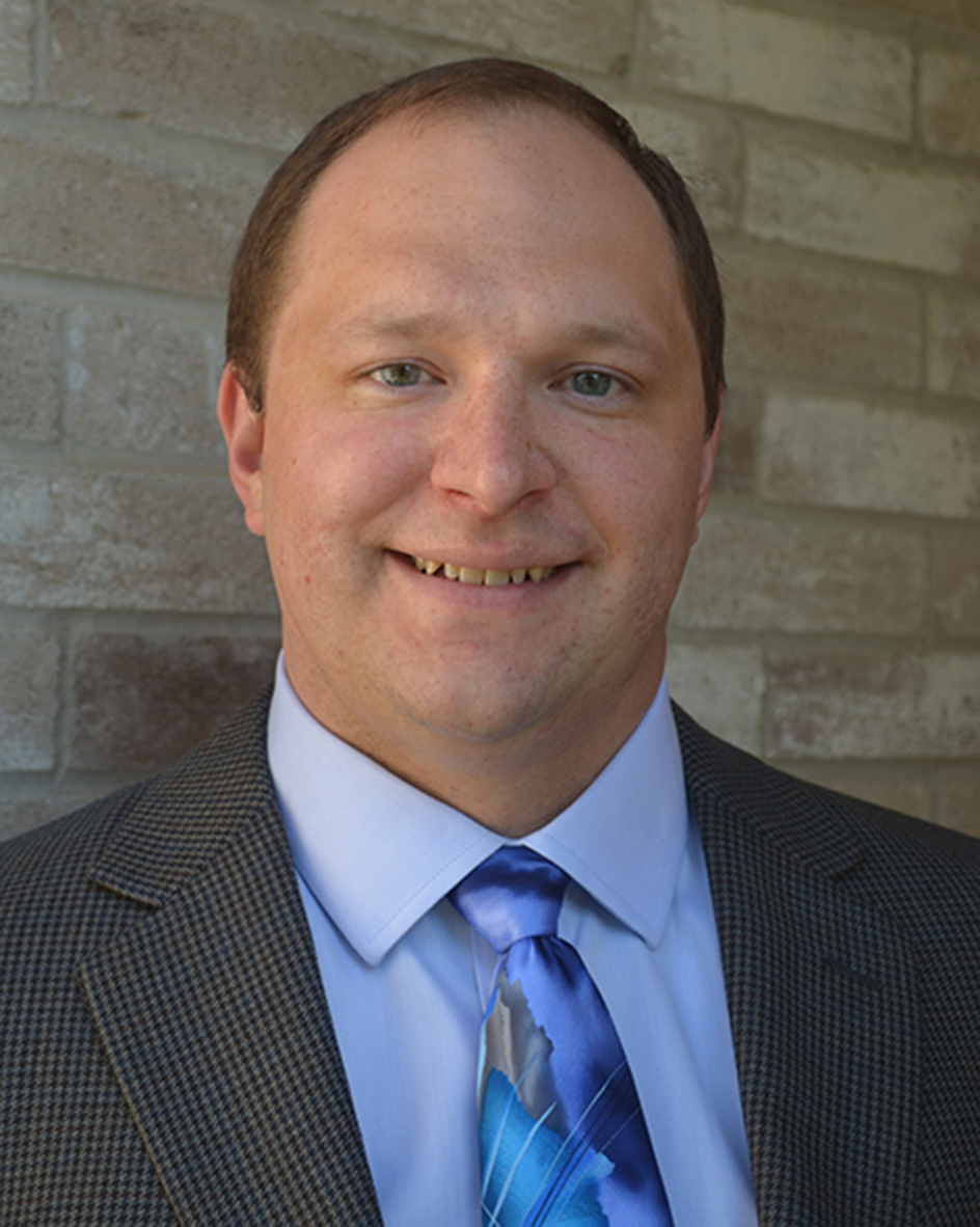 Marcus Sky Driver
Marcus Sky Driver
Post-Doctoral Researcher at the University of North Texas
I am currently working on projects for Theme 1 and Theme 3. For Theme 1, I am helping to grow ultrathin Cr2O3(0001) films on single domain Cu(111) substrates. We suspect that these films will be able to switch magnetic orientations with low applied voltage and significantly lower the required power for a broad range of spintronics devices. For Theme 3, we are growing hexagonal boron nitride (h-BN) and graphene/h-BN heterostructures with atomic layer epitaxy and molecular beam epitaxy to build tunnel junctions, spin valves, and other devices for testing.
My Ph.D. research focused on the chemical and electronic structure of amorphous hydrogenated boron carbide for use in neutron detection. Researchers at North Texas are also working on boron carbides, and I’ve been able to participate in some of their work. I’ve had multiple publications based on my boron nitride work and on C-SPIN-related research.
Like most scientists, I have a general curiosity about how things work. As an undergraduate, this quickly progressed into wanting to understand the physical, chemical and electronic properties of materials and how these properties could be used to produce useful devices. As a graduate student and a post-doc, research is exciting because when you start off, there is nothing but a blank substrate that is grown to some type of high precision in an epitaxial form. The high precision and care eventually adds up to an epitaxial multi-layered device. What’s fascinating is pulling all the properties of the various materials together to make a new device.
Membership in C-SPIN is very exciting because of the broad array of collaborative expertise on transport, magnetic measurements, and materials growth and characterization. I feel like I have contributed a significant amount to growing multilayer epitaxial h-BN for MTJs, but I also know that there is much more that needs to be done. Looking ahead, I hope to have a career that contributes significantly to materials and device development and production of spin-based and other nanoelectronic devices.
