

August 2017 Newsletter: Volume 4, Issue 3
A Message from the Director
We reviewed the exciting outcomes of Themes 1 and Theme 2 in previous newsletters, so Themes 4 and 5 are highlighted this quarter. Thank you to Steve Koester, Kaushik Roy, and Sachin Sapatnekar for their good Theme leadership.
As I was reading these brief histories of each Theme, I noticed that many “unexpected” breakthroughs arose from C-SPIN’s cross-disciplinary, multi-institutional vision, proving again that C-SPIN’s whole really is greater than the sum of its parts. Further proof of this is the recent review on the promising aspects of spin-based systems through C-SPIN’s vertical integration presented at DAC 2017. C-SPIN has truly been a one-of-a-kind research center in the computing electronics research and industry community – we should all be proud of our work together.
I’m also convinced that C-SPIN’s efforts have re-positioned U.S. academia back to a leading position on spintronic research for computing and memory. This could not have happened without the generous support of our STARnet sponsors and the great vision of engineering leaders from the US semiconductor industry. The unique connections that PIs, post-docs, and graduate students have made with our sponsors will benefit all parties.
Finally, I am highly pleased that much of the original C-SPIN research continues to stimulate a lot of new research around the world.
Thanks to Mike Lotti and Marie Rahne again for preparing this issue of the newsletter.
New Sputtering System Just in TimeA new tool to rapidly advance spintronic research
Industry’s loss has turned into C-SPIN’s gain. A virtually unused multi-chamber sputtering deposition system (MC-SD) is now in the University of Minnesota’s Nanocenter, nearly ready for industry and academic research.
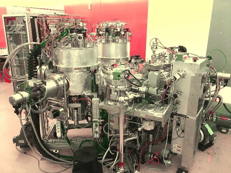 Figure 1. MC-SD sputtering system in a clean room at the UMN Nanocenter.
The MC-SD machine was originally bought by Hitachi Global Storage Technologies (HGST) for approximately $4M from Oerlikon Leybold Vacuum (OLV). Before HGST could use the MC-SD for advanced materials research, however, the company was bought by Western Digital in 2012 – just before Jian-Ping Wang submitted the original white paper for C-SPIN. Western Digital phased out the HGST research arm that used the sputtering system, so the system sat unused until this year.
When Jian-Ping Wang heard about the unused machine through industry connections, he began rallying donors. Soon C-SPIN, the University of Minnesota’s Office of the Vice President for Research, the Dean's Office of the College of Science and Engineering, and a few other sources had pledged $500,000, and the sputtering system was on its way to the Minnesota Nanocenter.
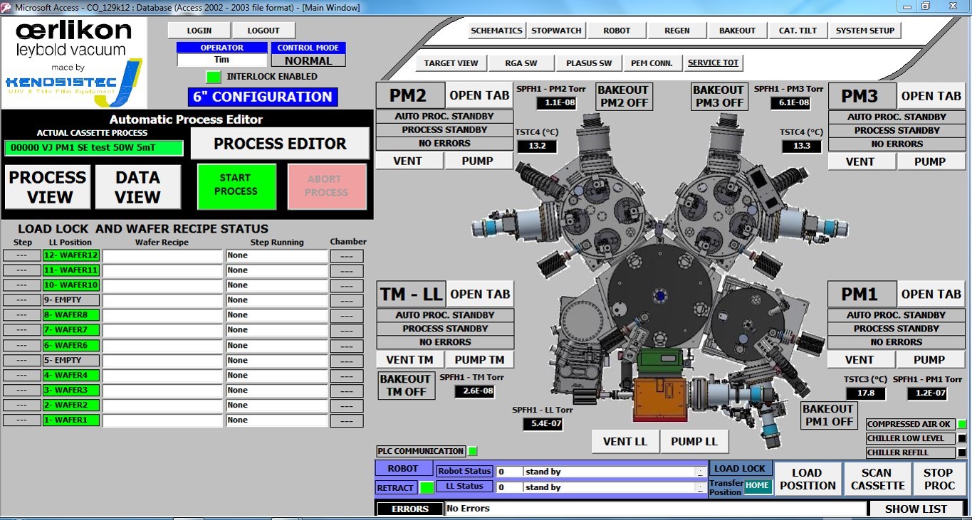 Figure 2. User interface of the MC-SD sputtering system.
“The incredible value of the deal made it easy to sell,” says Wang. “We were getting an industrial-level research tool for about 12 percent of the original purchase price. Moreover, we knew that plenty of academic and industry researchers outside of Minnesota would pay to use it.” Wang noted the special effort and leadership from Prof. Mos Kaveh, UMN’s Associate Dean of the College of Science and Engineering.
With two 4-sputter chambers – one for metals one for non-metals – the MC-SD system can produce a wide variety of high-quality samples on industry-standard wafers (from 1-8 inches) in a short amount of time. It can also produce dozens of samples at once with a good repeatability.
Figure 1 above is the user interface together with a top-down view of the MC-SD system, and figure 2 is a photograph of the system installed in a Minnesota Nanocenter cleaning room. The impressive specifications of the new system are listed in the table below.
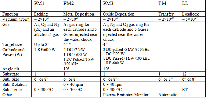 Table 1: The specifications of the MC-SD system.
*2 stronger magnets for magnetic materials deposition in PM2 and 1 strong magnet in PM3.
C-SPIN will wrap up its research in a few months, but it will still benefit from this system. Jian-Ping Wang’s group, for example, already plans to sputter SOT materials, Heusler alloys, and two different kind of MTJs for testing. Several companies have also expressed strong interest in using the system.
C-SPIN extends thanks for the good teamwork from Prof. Bin Ma, Dr. Junyang Chen, Thomas Peterson, Protyush Sahu, Mr. Jonathon Fink, Mr. Gary Olin, Mr. Corey Ngo, Mr. Carlo Aliberti and Mr. Simone Colucci, and the strong supporting team from AVP technologies and Kenosistec. Also thanks to Marie Rahne and Kyle Dukart for setting up a the user tracking system and website for this system. The MC-SD system is currently being calibrated and is expected to be fully operational at the beginning of October. If you are interested in using the system, please contact Marie L. Rahne for more information.
Looking Back, Looking Ahead: Theme 4
Not long after C-SPIN was named a SRC STARnet center, the original Theme 4 members had to be changed. Even with a semi-scramble by C-SPIN Director Jian-Ping Wang and new Theme 4 leader Steve Koester, most of the Theme’s research started 2-3 months after the Center officially opened in January 2013. On the plus side of that scramble, however, was the addition of PIs Geoffrey Beach (MIT) and Maxim Tsoi (Univ. Texas Austin) to the Theme 4 team.
Even after the addition of Beach and Tsoi, the Theme 4 goals didn’t change from the original proposal to STARnet:
- Develop new device concepts based upon new spintronic material properties. These materials included antiferromagnets, ferromagnets with perpendicular anisotropy, and materials with strong-spin orbit coupling.
- Develop a scalable, sub-20nm spin Hall MTJ that can be cascaded. This was, in essence, aimed at replacing binary CMOS devices with spintronic near-equivalents. Before 2013, such MTJs had only been developed in theory (by soon-to be C-SPIN PIs from Purdue).
- Control the direction and increase the transmission length of spin information. Both of these were closely connected to research in Theme 2 and involved the development of graphene and spin-to-optical and optical-to-spin information transfer. The goals: 10GB/sec that consumes 10fj/bit and 10μm spin diffusion length.
- Model non-volatile memory and logic devices and systems. This was a key goal for the entire Center, and it relied on partnership with Theme 5 and multiple materials development projects in other Themes.
Expected Progress
Theme 4 began – like the other C-SPIN Themes – with advances in measurement that lay the groundwork for other advances. In the first year, Chia-Ling Chien and Jian-Ping Wang developed new (and much more accurate) ways to measure the spin Hall angle of materials and interfaces. In the second year, Maxim Tsoi developed new methods for measuring antiferromagnetic (AFM) materials. In 2015, Supriyo Datta and his group published a groundbreaking paper in Scientific Reports that established quantitative and scalable modeling methodology for evaluating spintronic and nanomagnetic devices. These models are likely to be expanded and improved upon as more researchers use them and more spintronic materials and devices are developed.
Mo Li and Jian-Ping Wang’s work with spin-optical systems resulted in significant breakthroughs. By the end of year 3, their teams had achieved two versions of all-optical switching, one of which was with an MTJ with an “optical” layer whose switching behavior could be detected electrically. In the past year, the team has continued to develop MTJs and switch them with 500 fs laser pulses. The advantage of these systems is simple: their main components operate at the speed of light.
On the modeling front, Supriyo Datta and his team recently presented a new spintronic computing architecture – Probabilistic Spin Logic – that can perform highly complicated calculations both backwards and forwards. Importantly, the architecture is based on nanomagnets that already exist and function at room temperature. As with the 2015 Datta paper, this article will likely serve as a foundation for the testing and development of several new devices.
C-SPIN has led a comprehensive effort in the world to find a practical way to address the external field free SHE switching for MTJ and integrated devices. Thus far, Chia-Ling Chien, Kang Wang and Jian-Ping Wang have each proposed an innovative approach.
Unexpected Progress
Theme 4 surprise #1 has probably been skyrmions. Skyrmions had been identified before C-SPIN began, but Geoff Beach was the first to stabilize them so they could be measured and manipulated at room temperature. Smaller than 5 nm, they have proven to be stable and rapidly switchable at room temperature. Along with topological insulators, they are promising materials for future spin-based memory and logic.
Surprise #2 for Theme 4 is graphene. As graphene is one of the best spintronic channel materials in the world, C-SPIN researchers in Theme 2 and Theme 4 had planned on working with it from the beginning. It was thought that it would be an excellent material for all-spin logic, but Theme 4 researchers discovered that it’s even more valuable as a tunable spin channel. In other words, the distance spins travel in graphene can be changed by applying a control voltage. This property has allowed C-SPIN researchers to develop new ways of using graphene for computing systems – including neuromorphic systems – that are difficult to realize with traditional materials.
Surprise #3 is Maxim Tsoi’s demonstration of the world’s first electrically induced magnetization switching of an AFM oxide through a point-contact measurement. With more development, AFM materials may be crucial to a number of spintronic devices in the future.
A final surprise is Michael E. Flatté’s development of a completely new device concept based upon CSPIN’s pioneering effort on topological insulator spintronic materials from Theme 2 and the physics of magnetoelectric transduction. This approach uses a topological insulator – which has the highest efficiency of conversion of electric field to spin torque yet observed at room temperature – combined with a magnetic insulator to create an ultra-low-power spintronic switch. The insulator can be switched using an electric field, not a charge current, which dramatically reduces the power consumption for switching. Flatté performed theoretical calculations which show that this device can produce switching energies roughly 5 orders of magnitude lower than state-of-the-art CMOS. There are still some questions about this design. Further theoretical and experimental effort should be followed up.
Looking Ahead
Theme 4 PIs and their teams are currently working to publish all Theme 4 results so that other researchers in the field and in industry can further expand upon C-SPIN’s legacy.
What will that expansion look like? In computational research, Theme 4 efforts to develop neuromorphic computing (based on graphene, topological insulators, and other novel materials) will likely have enormous impact in the rapidly growing “artificial intelligence” industry and will, of course, spur plenty of further university research. Non-volatile, low-power memory – and possibly logic – will also likely benefit from C-SPIN’s advances in skyrmions, magnetic tunnel junctions, and anti-ferromagnetic materials. As for spin-optical devices, the possibilities are endless: sensors, defense-related applications, quantum computing, secure communications, and others.
Looking Back, Looking Ahead: Theme 5
In 2012, spintronics was seen as one of several technologies that could potentially provide new computational platforms for the post-CMOS era. The problem: MTJ-based memories and logic, all-spin logic (ASL) circuits for digital logic, and early preliminary structures for neuromorphic information processing had been proposed, but simulations showed that they either consumed high levels of power or processed information slowly.
Still, those theoretical conclusions were just that – theoretical. The sheer newness of spintronics as a major field of study meant that nobody really knew what nanomagnets could do for the computing industry. In fact, there were no robust spintronics-CMOS comparisons for spin injection efficiency, spin transfer, and numerous energy measures. So it was certainly possible that new spintronic architectures could spark a flurry of post-CMOS – or maybe even CMOS-enhancing – developments.
Theme 5 was included in the original C-SPIN proposal to address such issues. As the proposal stated, Theme 5 would be “the first ever integrated effort led by university designers to bring spin technology closer to practical reality with the direct support and guidance by semiconductor industry.”
Breakthroughs
The major breakthroughs for Theme 5 have come from close alignment with research in materials, devices, and underlying spintronic technologies:
- Neuromorphic computing. Clearly articulated as a goal in the original proposal, neuromorphic computing has moved much closer to reality through Theme 5 research. Novel circuits using domain wall based devices have resulted in orders-of-magnitude improvements in energy efficiency over prior CMOS-based techniques. These advances have the potential to enable rapid improvements in computer vision and recognition tasks that are at the heart of web search engines, automotive driver assistance systems, and autonomous robots.
- Logic speed and energy efficiency. Although it’s “common knowledge” that spin-based logic technology is not as developed as spin-based memory, C-SPIN, together with engineers from STARnet sponsors (e.g. Intel, Micron, etc.), has developed two paths that rival CMOS in speed and energy efficiency: 1) enhanced ASL using Heusler alloys, which demonstrates another positive result of the Center’s intentional integration from materials and devices to circuits and architectures, and 2) CoMET (Composite-input Magnetoelectric Technology), a new method of conveying spin information developed by Sachin Sapatnekar, Jian-Ping Wang, Chris Kim and their C-SPIN students.
- Benchmarking and comparative analysis. The development of new spintronic materials, devices, circuits, and architectures meant that new ways to measure and benchmark also had to be developed. A 2015 paper summarized the progress and challenges of spintronic research in light of CMOS performance. C-SPIN was the first to benchmark external-field-free Heusler alloys and SHE devices, and Sharon Hu contributed her expertise by developing ways to measure and compare non-volatile processors.
- Novel memory designs based on the spin Hall effect show major gains in energy efficiency over traditional STT-RAM.
- And a lot of other things…
- Development of stochastic neurons and spiking neural networks
- Architectures for solving NP-hard problems
- An ADC converter based on MTJs
- Development of non-volatile processors
- Architecture for SOT-domino-style spin logic
- Several designs for spin-CMOS hybrid systems.
Surprises
The original C-SPIN proposal noted that spintronics could potentially replace CMOS or complement CMOS. Nearly five years later, C-SPIN research has repeatedly shown that the real advantages of spintronic technology are best realized in complementing CMOS through the use of spin-specific circuits and architectures embedded within domain-specific accelerators. The best examples are neuromorphic computing and Probabilistic Spin Logic (PSL), two types of processing that can be done with CMOS but are orders of magnitude more efficient with architectures that take advantage of the unique properties of spintronic materials and devices.
Looking Ahead
A recent review on the promising aspects of spin-based systems, mostly stemming from Theme 5, was presented at DAC 2017.
The work of Theme 5 will likely bear fruit in three primary ways as industry and academic researchers continue to embrace spintronics:
- Deeper integration with CMOS. As CMOS technology becomes more difficult to scale, designers are likely to use spintronic architectures (like neuromorphic and PSL) for certain functions (like image recognition and probabilistic calculations), freeing up CMOS circuits for more traditional processing.
- Computation-in-Memory. Traditional computational models face a major speed/energy bottleneck with communication between the processor and memory, particularly for big-data applications. C-SPIN has been developing computational RAM (CRAM), which implements logic-in-memory using only minor modifications to a conventional memory array. By performing certain calculations in the RAM instead of in the processor, significant amounts of energy and time can be saved.
-
Approximate computing. A number of emerging applications do not require precise computational results, and spin-based logic is highly amenable to trading off computational accuracy for reduced circuit power. C-SPIN is exploring methods that use approximate computing to exploit this property.
Register Now for the 2017 Annual Review
The 2017 C-SPIN Annual Review will be held at the University of Minnesota September 27 - 28, 2017. Everyone planning to attend the annual review must REGISTER. Registration will close August 26, 2017. Please see the agenda page for more details about the review schedule. Details about the location of the review and nearby lodging options can be found on the C-SPIN website. We hope to see you again in Minneapolis!
Student and Post-Doc Profiles
Maghna Mankalale, Ph.D. Candidate, University of Minnesota
 Maghna Mankalale
I am currently working on developing novel low-power and high-speed spin-based logic devices, a project under Theme 5. The objective of this work is to use physics-based models to design and develop devices that can replace or complement existing CMOS transistors. In my first project, I worked on designing optimized all spin logic (ASL)-based standard logic gates like (N)AND, (N)OR, XOR, and inverter. I devised optimization techniques that considered the impact of layout factors during the design process. My techniques led to ASL gates that are up to 24% faster and up to 47% more energy efficient than previous versions. I also devised STEM, a novel two phase evaluation technique for ASL majority logic gates that provides up to 3.4x speed improvement and up to 6.9x improvement in energy dissipation over previous un-optimized ASL circuits.
I have also been working on CoMET, a magneto-electric based device, with my colleague Zhaoxin Liang and in collaboration with Prof. Jian-Ping Wang's group. We explored different material parameter combinations to determine that CoMET could deliver a speed of sub-100 ps with an energy dissipation of sub-100 aJ, a significant improvement over most other spintronic devices. I have also collaborated with Prof. Sharon Hu and Prof. Michael Niemier's groups at University of Notre Dame, who have explored the use of CoMET in nonvolatile processors and determined that it leads to a 2.3x improvement in energy over ASL devices. My research under C-SPIN has led to four first-author publications.
Prior to starting my PhD, I worked in the Design Automation group in IBM India for 6 years, where I worked on developing software tools for performing placement and routing of logic blocks during the design of an integrated chip (IC). This motivated me to work on challenging problems facing the IC design community. So when Prof. Sapatnekar offered me the PhD position to work on these problems in the area of spintronics, I grabbed it with both hands. The opportunity to work at the forefront of the beyond-CMOS revolution is truly exciting and I consider myself to be lucky to be a part of it.
I plan to apply for faculty positions, and I eagerly look forward to using the skills and expertise I’ve developed to research new computing and storage devices. In particular, I hope to continue to work on viable candidates for replacing today’s CMOS transistor-based ICs. I believe my experience using novel physics-based models to propose new spin-based devices, coupled with a background in circuit theory and automation, makes me uniquely qualified to take up this challenge and position myself as a key player in the post-silicon revolution. I also enthusiastically look forward to working with and mentoring new technical talent in this area.
Tobias Brown-Heft, Ph.D. Candidate, University California Santa Barbara
 Tobias Brown-Heft
I am currently working on MBE growth and characterization of atomic superlattices formed by pairs of Heusler materials for Theme 1. The project is based on some great theoretical work done a few years ago by Prof. Bill Butler’s group. They predicted that Heusler superlattices could produce a half-metal with perpendicular magnetic anisotropy and so would be an ideal contact for magnetoresistive memory devices. So far, the results are promising.
I have also been working on chemical and electrical analyses to determine how annealing affects Co2MnSi-based magnetic tunnel junction interfaces – another application of magnetic Heusler materials for spintronics. I have also worked on the synthesis and magnetic characterization of Co2TiGe epitaxial thin films, which are predicted to possess time-reversal breaking Weyl fermion states. We have a few publications on these topics.
I earned degrees in Physics and Chemistry before coming to UCSB in 2013. During my undergraduate years, I worked in an atom optics lab, so I didn’t have much experience with condensed matter systems. But I had two main goals: to create technical solutions to complex, real-world problems and to study lots of atoms at once, preferably magnetic ones. Needless to say, I’m achieving both at UCSB, so I enjoy my work immensely.
I expect to continue researching magnetic and spintronic systems in industry after I graduate. I want my contributions to make it into the hands of consumers. I’m excited about the future of computing technology. The steady progress toward complexity, reliability, and energy efficiency is changing the world every day, and being part of that really appeals to me.
